Optical Keyboard: Circuit Design
This guide will walk you through some concepts that will help you design a basic optical keyboard PCB. No special knowledge is assumed beyond engineering basics. The circuits used here are rudimentary and they will provide performance comparable to a mechanical keyboard. Low latency specialized circuits are not covered in this guide.


You can think of optical switches as apertures through which infra-red (IR) light (from LED) is allowed to pass through and shine on a phototransistor (PT). When switch is pressed the aperture window closes and stops the light from being irradiated on PT. PT generates current in response to light. A photodiode can also be used in place of phototransistor, but we will limit the discussion to PT. A PT is a combination of photodiode and another junction diode, making it a NPN transistor whose base is exposed to light. The current generated by PT has a near linear relationship with the amount of light shone on the base.
A PT is an analog device that produces current. This current needs to be converted to voltage at appropriate digital TTL levels before the ‘state’ of the switch (on/off) can be read by the GPIO (general purpose input-output) pin of a microcontroller. We use a passive device like a resistor to convert current to voltage. On the other hand, if you were to use a photodiode (which produces very small current) an active device like an OpAmp is needed to convert current to voltage (transimpedence).
We are interested in only two states (on/off) for digital operation. We are not interested in partial keypresses for instance (analog operation). So we drive the PT between saturation (on) and cutoff (off) states.
Circuit
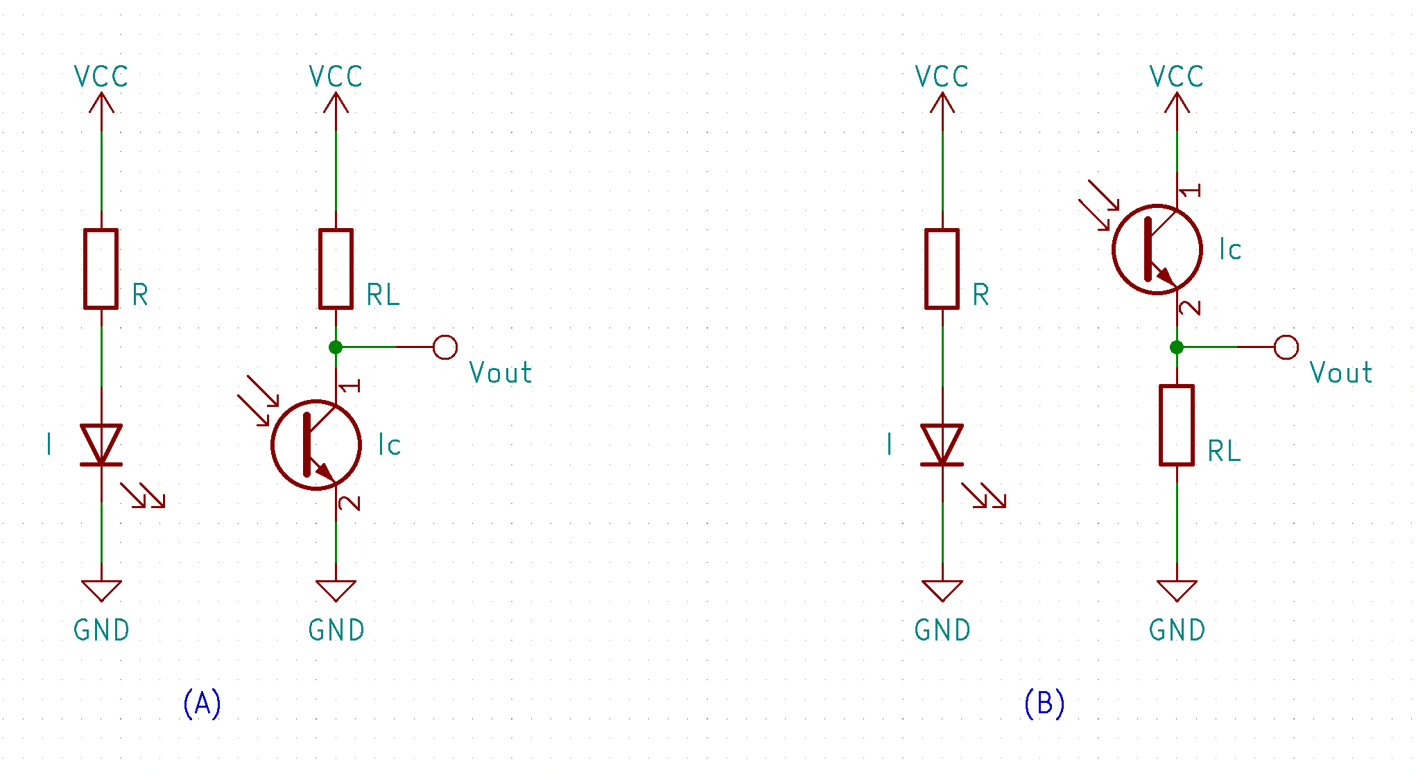
There are two ways you can measure voltage drop across PT. The circuit shown in Figure (A) is a common-emitter amplifier, with IR LED shown on left and PT on the right. Light input at the base causes the output (Vout) to decrease from high to low. If you were to connect Vout to the input pin of MCU it would read LOW to HIGH when switch is depressed. The circuit shown in Figure (B) is a common-collector amplifier with an output (Vout) increasing from low to high in response to light input. In this case MCU pin will read HIGH to LOW. For these circuits to operate in the switching mode, Vcc < RL × Ic, where Ic is the maximum anticipated current and Vcc is the supply voltage.
What are the values of R and RL?
Majority of current is consumed by the IR LED. First we have to determine how much current is available for each IR LED, and then we can use Ohm’s law to calculate R. As a USB ‘device’ a keyboard is allocated 500mA current. We can budget up to 300 mA for optical switches for instance, and use the rest for microcontroller and backlight. We can allocate the current budget to each IR LED based on the matrix we choose. This will become clear later. RL is chosen by trial-and-error such that multimeter reads TTL level voltage when switch is on/off. Value of RL depends on the brand/type of PT and amount of IR light falling on PT. Here are some values for Everlight IR12-21C/TR8 and PT12-21B/TR8 combo. Please do your own experiment to fine tune RL. You can also use 5V source directly from USB instead of 3V3 for powering IR LED.
For 3.3v:
| R | I | RL | Ic |
|---|---|---|---|
| 540 | 4.2 mA | 4k | 0.83 mA |
| 1.5k | 1.4 mA | 27k | 0.18 mA |
| 2.2k | 1.0 mA | 45k | 0.1 mA |
- Voltage across R is ~2.14V
- I = 2.14/R, and Ic ~ 3.3/RL
- R and RL are in ohms
Rise and Fall Time
Recall that a PT is also a transistor. Transistor provides current amplification but also brings its peculiarities. The time needed for PT to reach saturation and thereby rise the voltage (say from 0V to 3V) is called ‘rise’ time. More specifically, rise time is the time needed for PT to rise from 10% of LOW value to 90% of HIGH value. Similary ‘fall’ time is defined for the reverse situation. In addition, there is ‘storage’ time which is the time the transistor stays on even after the base current (in this case light incident on the base) has been removed. Storage+fall time is slightly larger than rise time because transistor junction behaves like a capacitor. The charge stored in the base junctions must be removed before the transistor will turn off. The deeper the saturation of transistor the longer the turn off time. Rise, storage and fall time of PT directly impacts the latency of a keyboard.
How quickly does a PT rise and fall? Here are some illustrative examples for a PT driven to saturation. The circuit is the common-emitter amplifier from above (A). Vcc is set at 3.3V. PT used is Everlight PT12-21B/TR8 and IR LED is IR12-21C/TR8. Rise and Fall times for various R and RL values are given below. The oscilloscope screens represent the items in the table. Green line represent the voltage drop across PT and yellow line is the voltage drop across IR LED. us/div number represents millisec per division (horizontal). Current across PT is not calculated since it is a much smaller value.
| R | IR LED Current | RL | Rise Time | Fall+Storage Time |
|---|---|---|---|---|
| 1k ohm | 2.3 mA | 30k ohm | ~250 us | ~300 us |
| 300 ohm | 7.5 mA | 4.5k ohm | ~100 us | ~100 us |
| 100 ohm | 20.2 mA | 1.8k ohm | ~20 us | ~20 us |
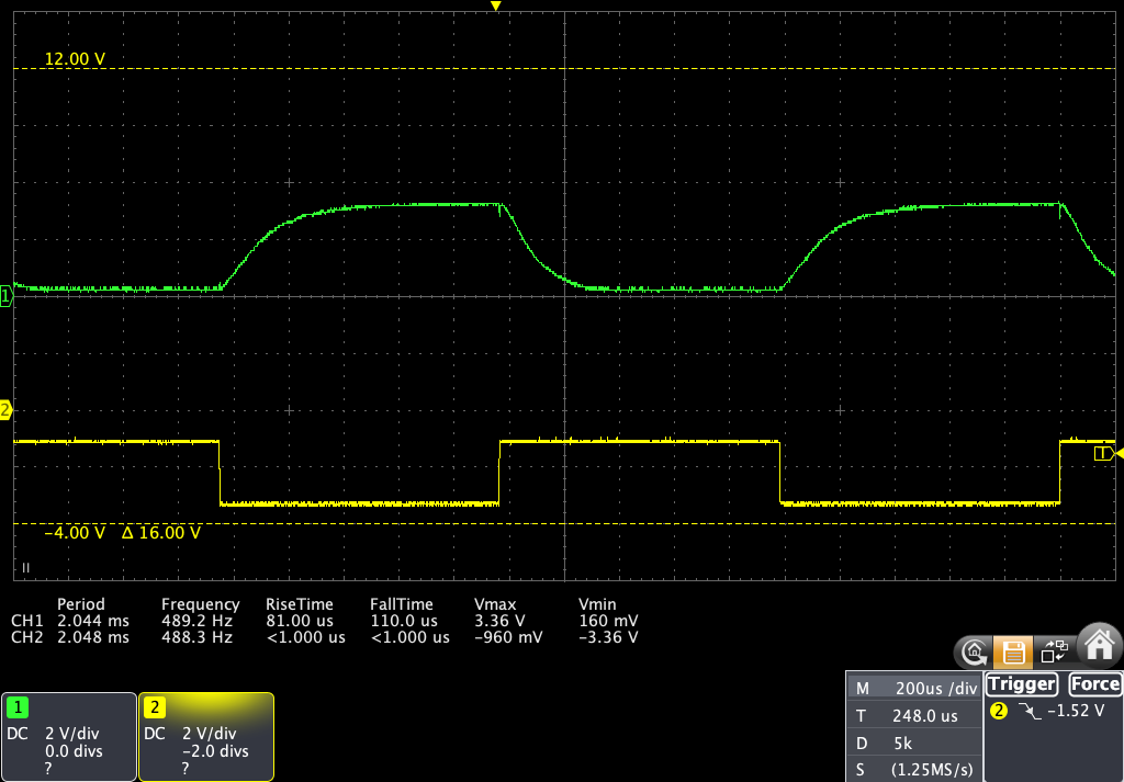
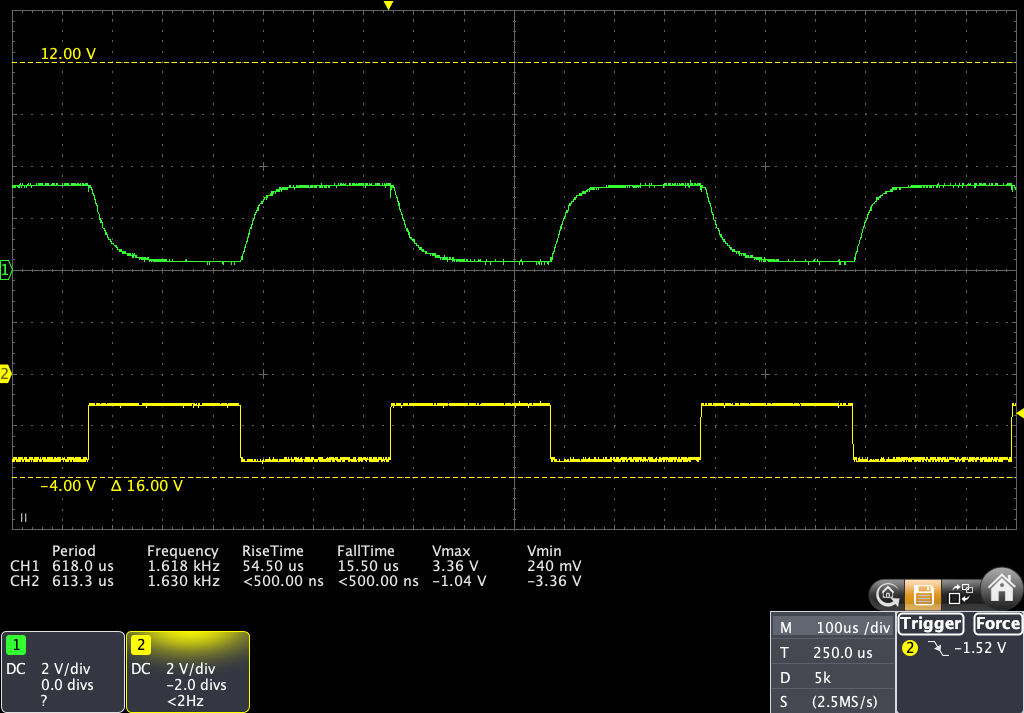
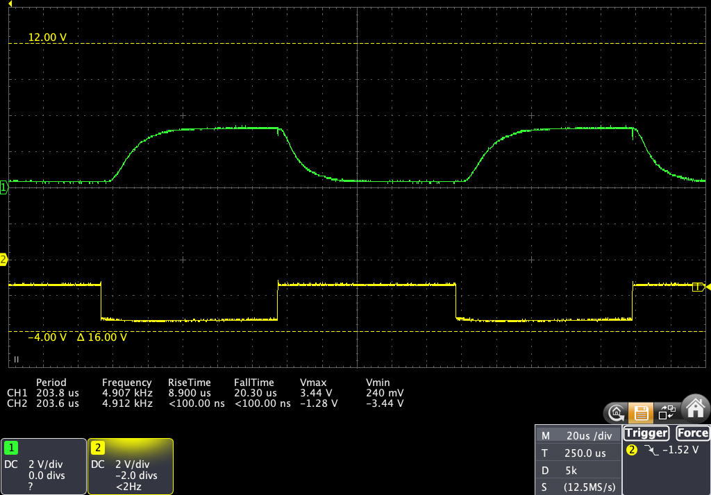
In the above pictures voltage values are inverted. ‘Rise’ is when yellow line goes from high to low, and vice versa. Rise and fall times are approximations eye-balled from oscilloscope plots.
It may appear execessive that at least 20mA current is needed to achieve rise time of 20us. But with minor modifications to the circuit it is possible to achieve 1us rise/fall time expending only a few mA current. Using photodiodes and OpAmps is not necessary.
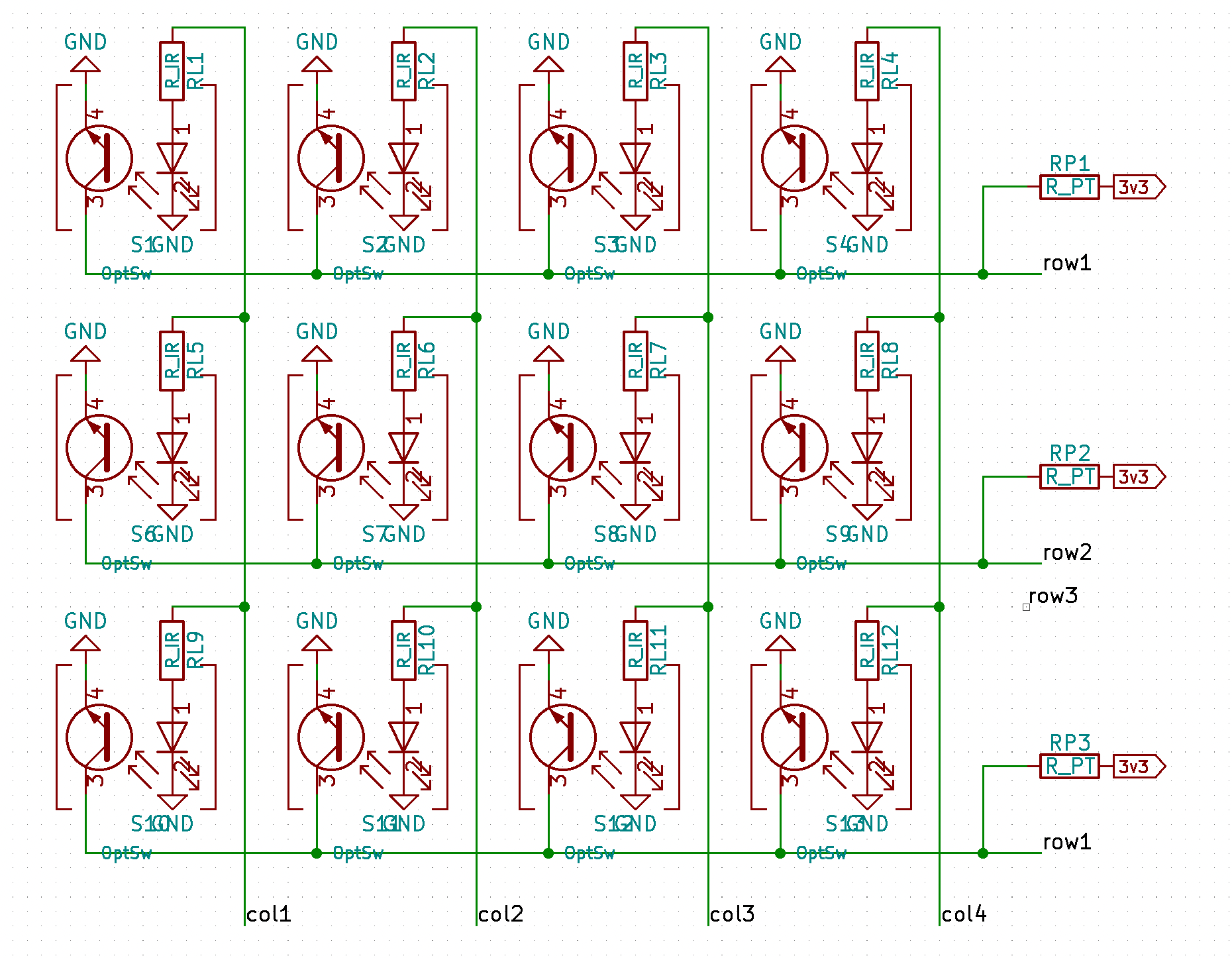
Optical Matrix
The total number of switches in a full-sized keyboard far exceed the number of digital pins available in a microcontroller for reading TTL voltage levels. We can solve this problem two ways: 1) Use a matrix arrangement where a single GPIO pin is connected to multiple PTs but only one of the PTs is ‘active’ at any given time, 2) Use a separate device like a multiplexer or shift register to read multiple PT voltages from a single GPIO pin. In the former case only a subset of IR LEDs are switched on at any given time (‘scanning’ the matrix). In the latter case all IR LEDs can be switched on and switch states can all be read at once. By now you may have already have some ideas about the matrix you want to design. Following section covers only basic information.
Optical matrix is not much different from matrix used for mechanical switches. You either select a column and read rows one by one, or vice versa.
Select Column and Read Rows
In this arrangement we switch on all IR LEDs in a give column and read PT values across rows. Pseudocode would look like this:
initialize GPIO pins

forever do:
    for column in all_columns do:
        select column  /* switch on power to column */
        delay          /* wait for rise time */
        for row in all_rows do:
            read row   /* read state of switch */
        unselect column /* switch off power to column */
        delay          /* wait for storage and fall time */

    compare matrix_state with matrix_state_from_previous_scan
    if above comparison returs true:
        copy matrix_state to matrix_state_from_previous_scan
        return matrix_state
To power IR LEDs in a column you can use a GPIO pin directly (set as OUTPUT). ARM based microcontrollers like RP2040 or STM32F4 can handle 20 mA current per pin (for a maximum of ~40 mA across all pins). If you have 5 columns you can supply 3.5 mA per IR LED (leaving 0.5 mA for PT).
Reading time is usually negligible compared to PT rise/fall time. A full matrix
scan will take approximately (rise_time + fall time) x number_of_columns.
Select Row and Read Columns
In this arrangement we select a row and read column pins one by one. A full
matrix scan will take (rise_time + fall_time) x number_of_rows. This is my
preferred arrangement since we can achieve higher scan rates. Rows can be
powered using a N-Mosfet acting as a low-side switch connected to a GPIO pin at
the gate. We can supply higher power to IR LED since we are not limited by GPIO
pin.
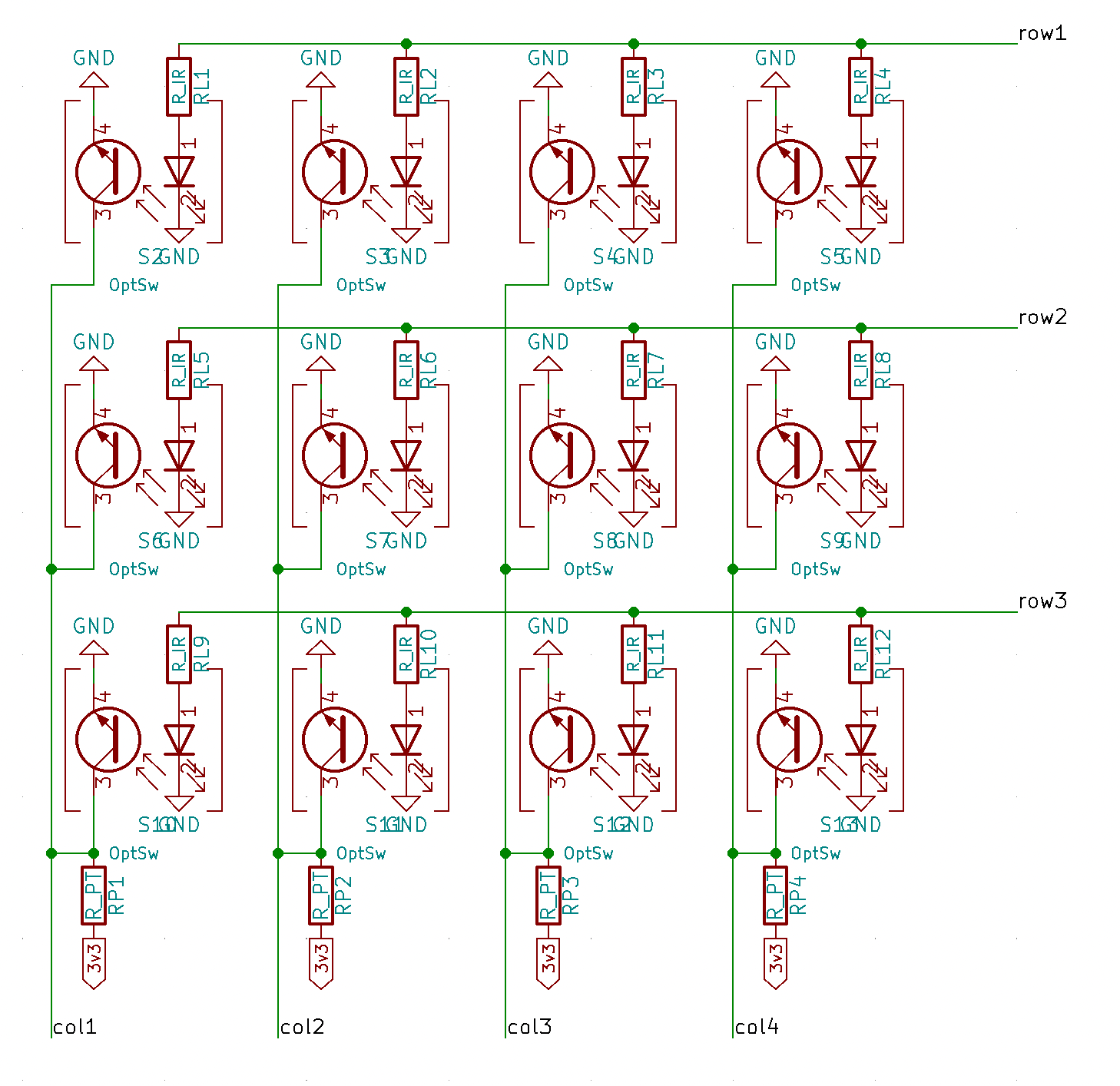
Note: To minimize power losses IR LEDs could be connected in series when possible. Modify the above schematic accordingly for your use-case. Voltage drop across IR LED (Vf) is typically 1.2V-1.3V. Using a 5V supply it is possible to connect 3 IR LEDs in series and still have headroom for regulation. LED forward voltage drop has inverse relationship with temperature. As LEDs heat up the forward voltage reduces resulting in more current. This causes further increase in temperature and could lead to thermal runaway. It is good to keep 20%-30% voltage headroom across resistor for proper regulation.
Optimization
One easy way you can increase the performance is by splitting the matrix into two. We can scan rows from each matrix alternately. This way when one matrix is waiting in ‘rise’ time, the other is waiting in ‘fall’ time. But storage time has to be accounted for each row separately. Latency is decreased by the same amount as rise time.
Using RP2040 (which has 30 GPIO pins) in a keyboard with 72 switches we can use 2 4x9 matrices, and we need 26 GPIO pins. Each row has 9 IR LEDs and each can be supplied with at least 20mA.
FS (full speed) USB supports 1 ms polling (1 kHz) while HS (high speed) USB supports 125us polling (8 kHz). Even though phototransistors are inherently slow it is possible to achieve ~8 kHz scan rate using PT without additional circuitry, while photodiodes in combination with OpAmps can generate square waves upto 100 kHz. Hopefully, this writeup kindled some curiousity in you about the workings of optical keyboards.
Optical Keyboards
- Optical keyboard with MX switches
- Optical keyboard with low profile switches
- Amoeba single switch pcb